(China (Mainland))

Product Summary
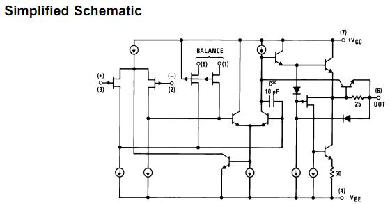
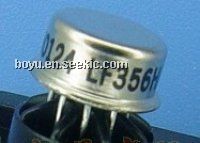
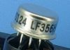
The LF356BH is a JFET input operational amplifier to incorporate well matched, high voltage JFETs on the same chip with standard bipolar transistors (BI-FET Technology). The LF356BH features low input bias and offset currents/low offset voltage and offset voltage drift, coupled with offset adjust which does not degrade drift or common-mode rejection. The LF356BH is also designed for high slew rate, wide bandwidth, extremely fast settling time, low voltage and current noise and a low 1/f noise corner. The applications of the LF356BH include Precision high speed integrators, Fast D/A and A/D converters, High impedance buffers and Wideband, low noise, low drift amplifiers.
Parametrics
LF356BH absolute maximum ratings: (1)Supply Voltage: ±22V; (2)Differential Input Voltage: ±40V; (3)Input Voltage Range: ±20V; (4)Output Short Circuit Duration: Continuous; (5)TJMAX: 100℃; (6)Power Dissipation at TA = 25℃: 670 mW; (7)Thermal Resistance (Typical), θJA: 130℃/W; (8)Storage Temperature Range: -65 to +150℃; (9)Soldering Information (Lead Temp.): 300℃; (10)ESD tolerance: 1000V.
Features
LF356BH features: (1)Replace expensive hybrid and module FET op amps; (2)Rugged JFETs allow blow-out free handling compared with MOSFET input devices; (3)Excellent for low noise applications using either high or low source impedance—very low 1/f corner; (4)Offset adjust does not degrade drift or common-mode rejection as in most monolithic amplifiers; (5)New output stage allows use of large capacitive loads (5,000 pF) without stability problems; (6)Internal compensation and large differential input voltage capability.
Diagrams