(China (Mainland))

Product Summary
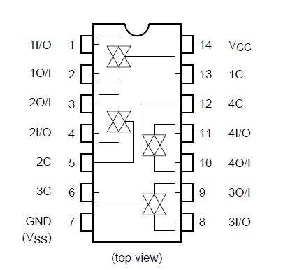
The tc74hc4066af(f) is a high speed CMOS quad bilateral switch fabricated with silicon gate C2MOS technology. The tc74hc4066af(f) consists of four independent high speed switches capable of controlling either digital or analog signals while maintaining the CMOS low power dissipation. Control input (C) is provided to control the switch. The tc74hc4066af(f) turns ON while the C input is high, and the switch turns OFF while low. All inputs are equipped with protection circuits against static discharge or transient excess voltage.
Parametrics
tc74hc4066af(f) absolute maximum ratings: (1)Supply voltage range VCC: - 0.5 to 13 V; (2)Control input voltage VIN: -0.5 to VCC + 0.5 V; (3)Switch I/O voltage VI/O: -0.5 to VCC + 0.5 V; (4)Control input diode current IIK: ±20 mA; (5)I/O diode current IOK: ±20 mA; (6)Switch through Current IOUT: ±25 mA; (7)DC VCC/ground current ICC: ±50 mA; (8)Power dissipation PD: 500 (DIP)(Note 2)/180 (SOP/TSSOP)mW; (9)Storage temperature Tstg: -65 to 150 °C.
Features
tc74hc4066af(f) features: (1)High speed: tpd = 7 ns (typ.)at VCC = 5 V; (2)Low power dissipation: ICC = 1 μA (max)at Ta = 25°C; (3)High noise immunity: VNIH = VNIL = 28% VCC (min); (4)Low on resistance: RON = 50 Ω (typ.)at VCC = 9 V; (5)High degree of linearity: THD = 0.05% (typ.)at VCC = 5 V; (6)Pin and function compatible with 4066B.
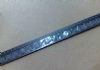
Diagrams