(China (Mainland))

Product Summary
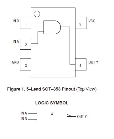
The mc74vhc1g08dft1 is an advanced high speed CMOS 2–input AND gate fabricated with silicon gate CMOS technology. The mc74vhc1g08dft1 achieves high speed operation similar to equivalent Bipolar Schottky TTL while maintaining CMOS low power dissipation. The mc74vhc1g08dft1 is composed of three stages, including a buffer output which provides high noise immunity and stable output.
Parametrics
mc74vhc1g08dft1 absolute maximum ratings: (1)DC Supply Voltage VCC: –0.5 to +7.0 V; (2)DC Input Voltage VIN: –0.5 to +7.0 V; (3)DC Output Voltage VCC = 0 High or Low State VOUT: –0.5 to 7.0 –0.5 to VCC + 0.5 V; (4)Input Diode Current IIK: 20 mA; (5)Output Diode Current (VOUT < GND; VOUT > VCC)IOK: +20 mA; (6)DC Output Current, per Pin IOUT: +25 mA; (7)DC Supply Current, VCC and GND ICC: +50 mA; (8)Power dissipation in still air, SC–88A PD: 200 mW; (9)Lead temperature, 1 mm from case for 10 s TL: 260 °C; (10)Storage temperature Tstg: –65 to +150 °C.
Features
mc74vhc1g08dft1 features: (1)High Speed: tPD = 3.5ns (Typ)at VCC = 5V; (2)Low Power Dissipation: ICC = 2mA (Max)at TA = 25°C; (3)Power Down Protection Provided on Inputs; (4)Balanced Propagation Delays; (5)Pin and Function Compatible with Other Standard Logic Families; (6)Latchup Performance Exceeds 300mA; (7)ESD Performance: HBM > 2000V; MM > 200V, CDM > 1500V.
Diagrams
| Image | Part No | Mfg | Description |  |
Pricing (USD) |
Quantity | ||||||||||||
|---|---|---|---|---|---|---|---|---|---|---|---|---|---|---|---|---|---|---|
 |
 MC74VHC1G08DFT1 |
|
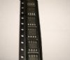
IC GATE AND SGL CMOS 2IN SOT353 |
Data Sheet |
Negotiable |
|
||||||||||||
 |
MC74VHC1G08DFT1G |
ON Semiconductor |
Gates (AND / NAND / OR / NOR) 2-5.5V Single AND 2-Input |
Data Sheet |
|
|
||||||||||||