(China (Mainland))

Product Summary
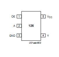
The 74lvc1g126gw is a high-performance, low-power, low-voltage, Si-gate CMOS device, superior to most advanced CMOS compatible TTL families. The input of the 74lvc1g126gw can be driven from either 3.3 V or 5V devices. The 74lvc1g126gw is fully specified for partial power-down applications using Ioff.
Parametrics
74lvc1g126gw absolute maximum ratings: (1) supply voltage Vcc: -0.5 to +6.5V; (2) input diode current IIK: -50mA; (3) input voltage VI: -0.5 to +6.5V; (4) output diode current IOK: ±50mA (Vo>Vcc or Vo<0 V) ; (5) output voltage Vo: -0.5 to Vcc +0.5V (enable mode) , -0.5 to 6.5V (disable mode) , 6.5V (Power-down mode) ; (6) output source or sink current: ±50mA (Vo=0 to Vcc); (7) VCC or GND current, Icc, IGND: ±100mA; (8) storage temperature Tstg: -65 to +150°C; (9) power dissipation Ptot: 250mW ( Tamb=-40 to +125°C) .
Features
74lvc1g126gw features: (1) Wide supply voltage range from 1.65 V to 5.5V; (2) High noise immunity; (3) Complies with JEDEC standard; (4) ±24mA output drive (Vcc=3.0V) ; (5) CMOS low power consumption; (6) Latch-up performance exceeds 250mA; (7) Direct interface with TTL levels; (8) Inputs accept voltages up to 5V; (9) Multiple package options; (10) ESD protection.
Diagrams
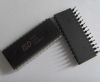
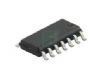
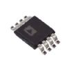
| Image | Part No | Mfg | Description |  |
Pricing (USD) |
Quantity | ||||||||||||
|---|---|---|---|---|---|---|---|---|---|---|---|---|---|---|---|---|---|---|
 |
 74LVC1G126GW,125 |
NXP Semiconductors |
Buffers & Line Drivers 3.3V PICOGATE BUS |
Data Sheet |
|
|
||||||||||||
|
74LVC1G126GW,165 |
NXP Semiconductors |
Buffers & Line Drivers BUS BUF/LINE 3-STATE |
Data Sheet |
Negotiable |
|
||||||||||||
|
74LVC1G126GW-G |
NXP Semiconductors |
Buffers & Line Drivers 3.3V PICOGATE BUS BUFFER/LINE |
Data Sheet |
Negotiable |
|
||||||||||||