(China (Mainland))


Product Summary
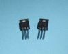
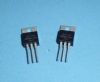
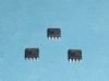
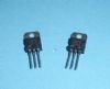
The fdc6312p is a P-Channel 1.8V specified MOSFET. It produced using Fairchild Semiconductors advanced PowerTrench process that has been especially tailored to minimize on-state resistance and yet maintain low gate charge for superior switching performance. It is ideal for: (1)Power management; (2)Load switch.
Parametrics
fdc6312p absolute maximum ratings: (1)VDSS Drain-Source Voltage: –20 V; (2)VGSS Gate-Source Voltage: ±8 V; (3)ID Drain Current – Continuous (Note 1a): –2.3 A; (4)Power Dissipation for Single Operation (Note 1a): 0.96 W; (5)TJ, TSTG Operating and Storage Junction Temperature Range: -55 to +150 °C.
Features
fdc6312p features: (1)–2.3 A, –20 V. RDS(ON)= 115 mΩ @ VGS = –4.5 V; RDS(ON)= 155 mΩ @ VGS = –2.5 V; RDS(ON)= 225 mΩ @ VGS = –1.8 V.; (2)High performance trench technology for extremely low RDS(ON); (3)SuperSOTTM-6 package: small footprint (72% smaller than standard SO-8); low profile (1mm thick).
Diagrams

| Image | Part No | Mfg | Description |  |
Pricing (USD) |
Quantity | ||||||||||||
|---|---|---|---|---|---|---|---|---|---|---|---|---|---|---|---|---|---|---|
 |
 FDC6312P |
Fairchild Semiconductor |
MOSFET SSOT-6 P-CH DUAL |
Data Sheet |
|
|
||||||||||||
 |
FDC6312P_Q |
Fairchild Semiconductor |
MOSFET SSOT-6 P-CH DUAL |
Data Sheet |
Negotiable |
|
||||||||||||