(China (Mainland))

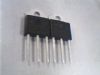
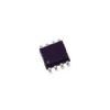
Product Summary
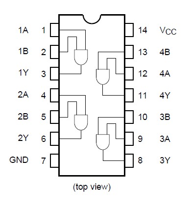
The tc74vhc132ft is an advanced high speed CMOS 2-INPUT AND GATE fabricated with silicon gate C2MOS technology. The tc74vhc132ft achieves the high speed operation similar to equivalent Bipolar Schottky TTL while maintaining the CMOS low power dissipation. The internal circuit is composed of 4 stages including buffer output, which provide high noise immunity and stable output. An input protection circuit ensures that 0 to 5.5 V can be applied to the input pins without regard to the supply voltage. The tc74vhc132ft can be used to interface 5 V to 3 V systems and two supply systems such as battery back up. This circuit prevents device destruction due to mismatched supply and input voltages.
Parametrics
tc74vhc132ft absolute maximum ratings: (1)Supply voltage range: -0.5 to 7.0 V; (2)DC input voltage: -0.5 to 7.0 V; (3)DC output voltage: -0.5 to VCC + 0.5 V; (4)Input diode current: -20 mA; (5)Output diode current: ±20 mA; (6)DC output current: ±25 mA; (7)DC VCC/ground current: ±50 mA; (8)Power dissipation: 180 mW; (9)Storage temperature: -65 to 150 °C.
Features
tc74vhc132ft features: (1)High speed: tpd = 4.3 ns (typ.)at VCC = 5 V; (2)Low power dissipation: ICC = 2 μA (max)at Ta = 25°C; (3)High noise immunity: VNIH = VNIL = 28% VCC (min); (4)Power down protection is provided on all inputs.; (5)Balanced propagation delays: tpLH - tpHL; (6)Wide operating voltage range: VCC (opr)= 2 V to 5.5 V; (7)Low noise: VOLP = 0.8 V (max); (8)Pin and function compatible with 74ALS132.
Diagrams