(China (Mainland))

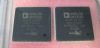
Product Summary
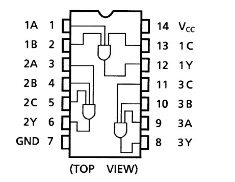
The TC74HC11AF is a high speed CMOS 3-input and gate fabricated with silicon gate C2MOS technology. The TC74HC11AF achieves the high speed operation similar to equivalent LSTTL while maintaining the CMOS low power dissipation. The internal circuit is composed of 4 stages including a buffer output, which provide high noise immunity and stable output. All inputs are equipped with protection circuits against static discharge or transient excess voltage.
Parametrics
TC74HC11AF absolute maximum ratings: (1)Supply voltage range, VCC: −0.5 to 7 V; (2)DC input voltage, VIN: −0.5 to VCC + 0.5 V; (3)DC output voltage, VOUT: −0.5 to VCC + 0.5 V; (4)Input diode current, IIK: ±20 mA; (5)Output diode current, IOK: ±20 mA; (6)DC output current, IOUT: ±25 mA; (7)DC VCC/ground current, ICC: ±50 mA; (8)Power dissipation, PD: 500 mW; (9)Storage temperature, Tstg: −65 to 150 °C.
Features
TC74HC11AF features: (1)High speed: tpd = 7 ns (typ.)at VCC = 5 V; (2)Low power dissipation: ICC = 1 μA (max)at Ta = 25°C; (3)High noise immunity: VNIH = VNIL = 28% VCC (min); (4)Output drive capability: 10 LSTTL loads; (5)Symmetrical output impedance: |IOH| = IOL = 4 mA (min); (6)Balanced propagation delays: tpLH ∽ tpHL; (7)Wide operating voltage range: VCC (opr)= 2 to 6 V; (8)Pin and function compatible with 74LS11.
Diagrams