(China (Mainland))

Product Summary
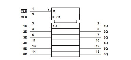
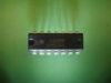
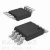
The sn74hc174ansr is a monolithic positive-edge-triggered D-type flip-flop have a direct clear (CLR) input. Information at the data (D) inputs meeting the setup time requirements is transferred to the outputs on the positive-going edge of the clock (CLK) pulse. Clock triggering occurs at a particular voltage level and is not directly related to the transition time of the positive-going edge of CLK. When CLK is at either the high or low level, the D input has no effect at the output.
Parametrics
sn74hc174ansr absolute maximum ratings: (1)Supply voltage range, VCC: –0.5 V to 7 V; (2)Input clamp current, I IK (VI < 0 or VI > VCC)(see Note 1): ±20 mA; (3)Output clamp current, IOK (VO < 0 or VO > VCC)(see Note 1): ±20 mA; (4)Continuous output current, IO (VO = 0 to VCC): ±25 mA; (5)Continuous current through VCC or GND: ±50 mA; (6)Package thermal impedance, θJA (see Note 2): D package 113: °C/W; N package 78 °C/W; (7)Storage temperature range, Tstg: –65 °C to 150°C.
Features
sn74hc174ansr features: (1)Contain Six Flip-Flops With Single-Rail Outputs; (2)Applications Include: Buffer/Storage Registers; Shift Registers; Pattern Generators; (3)Package Options Include Plastic Small-Outline (D)and Ceramic Flat (W)Packages, Ceramic Chip Carriers (FK), and Standard Plastic (N)and Ceramic (J)300-mil DIPs.
Diagrams