(China (Mainland))


Product Summary
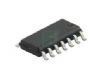
The mx29f200ctti-90g is a 2-mega bit, single 5 Volt Flash memory. The mx29f200ctti-90g is organized as 1M word × 16 or 2M byte × 8 MXIC’s Flash memories offer the most cost-effective and reliable read/write non-volatile random access memory. The mx29f200ctti-90g is packaged in 44-pin SOP and 48-pin TSOP. The mx29f200ctti-90g is designed to be reprogrammed and erased in-system or in-standard EPROM programmers. The standard the mx29f200ctti-90g offers access time as fast as 55ns, allowing operation of high-speed microprocessors without wait states. To eliminate bus contention, the mx29f200ctti-90g has separate chip enable (CE#) and output enable (OE#) controls.
Parametrics
mx29f200ctti-90g absolute maximum ratings: (1)Ambient Operating Temperature: -40 to 85 ℃; (2)Ambient Temperature with Power Applied: -55 to 125 ℃; (3)Storage Temperature: -65 to 125 ℃; (4)Applied Input Voltage: -0.5 V to 7.0 V; (5)Applied Output Voltage: -0.5 V to 7.0 V; (6)VCC to Ground Potential: -0.5 V to 7.0 V; (7)A9: -0.5 V to 13.5 V.
Features
mx29f200ctti-90g features: (1)5.0V±10% for read, erase and write operation; (2)131072 × 16/262144 × 8 switchable; (3)Fast access time: 55/70/90ns; (4)Compatible with mx29f200ctti-90g device; (5)Low power consumption; (6)Command register architecture; (7)Auto Erase (chip & sector) and Auto Program; (8)Status Reply; (9)Ready/Busy# pin; (10)Compatibility with JEDEC standard; (11)Sector protection; (12)Sector protect/chip unprotect for 5V only system; (13)100,000 minimum erase/program cycles; (14)Latch-up protected to 100 mA from -1V to VCC+1V; (15)Boot Code Sector Architecture; (16)Low VCC write inhibit is equal to or less than 3.2V; (17)Erase suspend/ Erase Resume; (18)Hardware reset pin; (19)20 years data retention; (20)Package type: 44-pin SOP.
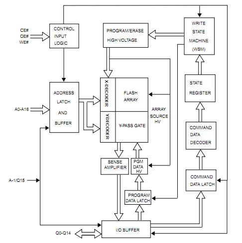
Diagrams