(China (Mainland))


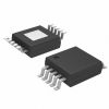
Product Summary
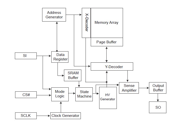
The mx25l512mc-12g is a CMOS 524,288 bit serial flash memory, which is configured as 65,536 x 8 internally. The mx25l512mc-12g features a serial peripheral interface and software protocol allowing operation on a simple 3-wire bus. The three bus signals are a clock input (SCLK), a serial data input (SI), and a serial data output (SO). SPI access to the device is enabled by CS# input. The mx25l512mc-12g provide sequential read operation on whole chip. When the device is not in operation and CS# is high, it is put in standby mode and draws less than 10uA DC cur­rent. The mx25l512mc-12g utilize MXIC proprietary memory cell, which reliably stores memory contents even after 100,000 program and erase cycles.
Parametrics
mx25l512mc-12g absolute maximum ratings: (1)Ambient operating temperature. Industrial grade: -40°C to 85°C; Commercial grade: 0°C to 70°C; (2)Storage temperature: -55°C to 125°C; (3)Applied input voltage: -0.5V to 4.6V; (4)Applied output voltage: -0.5V to 4.6V; (5)VCC to ground potential: -0.5V to 4.6V.
Features
mx25l512mc-12g features: (1)Serial peripheral interface (SPI)compatible: Mode 0 and Mode 3; (2)524,288 x 1 bit structure; (3)16 equal sectors with 4K byte each: Any sector can be erased individually; (4)Single power supply operation: 2.7 to 3.6 volt for read, erase, and program operations; (5)Latch-up protected to 100mA from -1V to Vcc +1; (6)High performance: Fast access time: 85MHz serial clock (15pF + 1TTL Load)and 66MHz serial clock (30pF + 1TTL Load); Fast program time: 1.4ms(typ.)and 5ms(max.)/page (256-byte per page); Fast erase time: 60ms(typ.)and 120ms(max.)/sector (4K-byte per sector); 1s(typ.)and 2s(max.)/chip(512Kb); (7)Low power consumption: Low active read current: 12mA(max.)at 85MHz, 8mA(max.)at 66MHz and 4mA(max.)at 33MHz; Low active programming current: 15mA (max.); Low active erase current: 15mA (max.); Low standby current: 10uA (max.)Deep power-down mode 1uA (typical); (8)Minimum 100,000 erase/program cycles.
Diagrams