(China (Mainland))

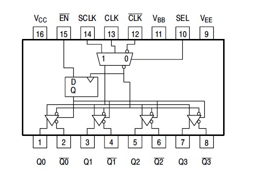
Product Summary
The MC10EL15DR2 is a low skew 1:4 clock distribution chip designed explicitly for low skew clock distribution applications. The VBB pin, an internally generated voltage supply, is available to this device only. For single-ended input conditions, the unused differential input is connected to VBB as a switching reference voltage. VBB may also rebias AC coupled inputs. When used, decouple VBB and VCC via a 0.01 μF capacitor and limit current sourcing or sinking to 0.5 mA. When not used, VBB should be left open.
Parametrics
MC10EL15DR2 absolute maximum ratings: (1)PECL Mode Power Supply: 8 V; (2)NECL Mode Power Supply: -8 V; (3)PECL Mode Input Voltage: 6 V; (4)NECL Mode Input Voltage: -6 V; (5)Output Current Continuous: 50 mA; (6)Output Current Surge: 100 mA; (7)VBB Sink/Source: ± 0.5 mA; (8)Operating Temperature Range: -40 to +85 °C; (9)Storage Temperature Range: -65 to +150 °C; (10)Thermal Resistance (Junction-to-Ambient)0 lfpm: 130 °C/W; (11)Thermal Resistance (Junction-to-Ambient)500 lfpm: 75 °C/W; (12)Thermal Resistance (Junction-to-Case): 33 to 36 °C/W; (13)Wave Solder Pb: 265 °C; (14)Wave Solder Pb-Free: 265 °C.
Features
MC10EL15DR2 features: (1)50 ps Output-to-Output Skew; (2)Synchronous Enable/Disable; (3)Multiplexed Clock Input; (4)PECL Mode Operating Range: VCC = 4.2 V to 5.7 V with VEE = 0 V; (5)NECL Mode Operating Range: VCC = 0 V with VEE = -4.2 V to -5.7 V; (6)Internal Input Pulldown Resistors on CLKs, SCLK, SEL, and EN.; (7)Pb-Free Packages are Available.
Diagrams
| Image | Part No | Mfg | Description |  |
Pricing (USD) |
Quantity | ||||||||||
|---|---|---|---|---|---|---|---|---|---|---|---|---|---|---|---|---|
 |
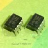
 MC10EL15DR2 |
ON Semiconductor |
Clock Drivers & Distribution 5V ECL 1:4 Diff |
Data Sheet |
Negotiable |
|
||||||||||
|
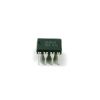
MC10EL15DR2G |
ON Semiconductor |
Clock Drivers & Distribution 5V ECL 1:4 Diff Clock Distribution |
Data Sheet |
|
|
||||||||||