(China (Mainland))

Product Summary
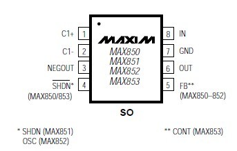
The max850esa(c70673) low-noise, inverting, chargepump power supply is ideal for biasing GaAsFETs in cellular telephone transmitter amplifiers. The max850esa(c70673) offers both preset (-4.1V) and adjustable (-0.5V to -9.0V) output voltages. The max850esa(c70673) uses an external positive control voltage to set the negative output voltage. Input voltage range for all four devices is 4.5V to 10V. Output current is 5mA. Applications are (1)Cellular Phones; (2)Negative Regulated Power Supplies; (3)Personal Communicators, PDAs; (4)Wireless Data Loggers; (5)Continuously Adjustable GaAsFET Bias; (6)LCD-Bias Contrast Control.
Parametrics
max850esa(c70673) absolute maximum ratings: (1)Supply Voltage, VIN to GND : -0.3V to 10.5V; (2)VNEGOUT to GND: -10.5V to 0.3V; (3)VIN to VNEGOUT : -0.3V to 21V; (4)VOUT to GND (Note 1): VNEGOUT to 0.3V; (5)SHDN or OSC (pin 4)Voltage to GND: -0.3V to (VIN + 0.3V); (6)Continuous Power Dissipation (TA = +70°C)SO (derate 5.88mW/°C above +70°C): 471mW; (7)Operating Temperature Ranges: -40°C to +85°C; (8)Storage Temperature Range : -65°C to +160°C; (9)Lead Temperature (soldering, 10sec): +300°C.
Features
max850esa(c70673) features: (1)Fixed -4.1V or Adjustable -0.5V to -9V Output at 5mA; (2)4.5V to 10V Input Voltage Range; (3)2mVp-p Output Voltage Ripple (MAX850–MAX852)1mVp-p Output Voltage Ripple (MAX853); (4)100kHz Charge-Pump Switching Frequency; (5)External Synchronizing Clock Input (MAX852); (6)Logic-Level Shutdown Mode: 1μA Max Over Temperature; (7)Low Cost, 8-Pin SO Package.
Diagrams