(China (Mainland))

Product Summary
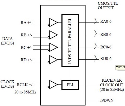
The THC63LVDF84A is a host-lcd panel interface receiver. It supports wide VCC range(2.5~3.6V). At single 2.5V supply, the device reduces EMI and power consumption. The THC63LVDF84A receiver converts the four LVDS(Low Voltage Differential Signaling) data streams back into 28bits of CMOS/TTL data with falling edge clock. At a transmit clock frequency of 85MHz, 28bits of RGB data and 4bits of LCD timing and control data (HSYNC, VSYNC, CNTL1, CNTL2) are transmitted at a rate of 2.3Gbps. Also the THC63LVDF84A receiver converts the three LVDS data streams back into 21bits of CMOS/TTL data with falling edge clock. At a transmit clock frequency of 85MHz, 21bits of RGB data and 4bits of LCD timing and control data (HSYNC, VSYNC, CNTL1, CNTL2) are transmitted at a rate of 1.78Gbps.
Parametrics
THC63LVDF84A absolute maximum ratings: (1)Supply Voltage (Vcc): -0.3 to +4V; (2)CMOS/TTL Input Voltage: -0.3 to (Vcc + 0.3V); (3)CMOS/TTL Output Voltage: -0.3V to (Vcc + 0.3V); (4)LVDS Receiver Input Voltage: -0.3V to (Vcc + 0.3V); (5)Junction Temperature: +125℃; (6)Storage Temperature Range: -55 to +150℃; (7)Resistance to soldering heat: +260 /10sec; (8)Maximum Power Dissipation 25: 0.5W.
Features
THC63LVDF84A features: (1)Wide VCC range: 2.5~3.6V; (2)Wide dot clock range: 20-85MHz suited for VGA,SVGA, XGA and SXGA (VCC=3.0~3.6V); (3)Wide dot clock range: 20-70MHz suited for VGA,SVGA, XGA and SXGA (VCC=2.5V~3.6V); (4)PLL requires No external components; (5)Rx power consumption < 80mW VCC 2.5V,65MHz Grayscale; (6)Power-Down Mode; (7)Low profile 56 Lead or 48 Lead TSSOP Package; (8)Pin compatible with THC63LVDF84A/F64A.
Diagrams