(China (Mainland))


Product Summary
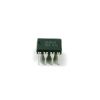
The OR2C06A-3S208I 2 SRAM-based FPGA is an enhanced version of the ATT2C/2T architecture. The OR2C06A-3S208I includes patented architectural enhancements that make functions faster and easier to design while conserving the use of PLCs and routing resources. The OR2C06A-3S208I provides a balanced mix of logic and routing that allows a higher utilized gate/PFU than alternative architectures. The routing resources carry logic signals between PFUs and I/O pads. The routing in the PLC is symmetrical about the horizontal and vertical axes. This improves routability by allowing a bus of signals to be routed into the PLC from any direction.
Parametrics
OR2C06A-3S208I absolute maximum ratings: (1)Storage Temperature Tstg: –65 to 150 °C; (2)Supply Voltage with Respect to Ground VDD: –0.5 to 7.0 V; (3)VDD5 Supply Voltage with Respect to Ground (OR2TxxA)VDD5 VDD: 7.0 V; (4)Input Signal with Respect to Ground OR2TxxA only: –0.5 to VDD + 0.3 VDD5 + 0.3 V; (5)Signal Applied to High-impedance Output OR2TxxA only: –0.5 VDD + 0.3 VDD5 + 0.3 V; (6)Maximum Soldering Temperature: 260 °C; (7)Input Leakage Current IL VDD = Max, VIN = VSS or VDD: –10 to 10 μA.
Features
OR2C06A-3S208I features: (1)High density (up to 43,200 usable, logic-only gates; or 99,400 gates including RAM); (2)Up to 480 user I/Os (OR2TxxA and OR2TxxB I/Os are 5 V tolerant to allow interconnectioto both 3.3 V and 5 V devices, selectable oa per-pibasis); (3)Four 16-bit look-up tables and four latches/flip-flops per PFU, nibble-oriented for implementing 4-, 8-, 16-, and/or 32-bit (or wider)bus structures; (4)Eight 3-state buffers per PFU for on-chip bus structures; (5)Upward bit stream compatible with the ORCA ATT2Cxx/ ATT2Txx series of devices; (6)Pinout-compatible with new ORCA Series 3 FPGAs; (7)TTL or CMOS input levels programmable per pifor the OR2CxxA (5 V)devices; (8)Individually programmable drive capability: 12 mA sink/6 mA source or 6 mA sink/3 mA source; (9)Built-iboundary sca(IEEE1149.1 JTAG)and 3-state all I/O pins, (TS_ALL)testability functions; (10)Multiple configuratiooptions, including simple, low pincount serial ROMs, and peripheral or JTAG modes for insystem programming (ISP); (11)Full PCI bus compliance for all devices.
Diagrams