(China (Mainland))


Product Summary
The G2996F1U is a linear regulator designed to meet the JEDEC SSTL-18 ,SSTL-2 and SSTL-3 (Series Stub Termination Logic) specifications for termination of DDR-SDRAM. It contains a high-speed operational amplifier that provides excellent response to the load transients. The G2996F1U can deliver 1.5A/0.9A continuous current and transient peaks up to 3A/1.8A in the application as required for DDRI/II-SDRAM termination. With an independent VSENSE pin, the G2996F1U can provide superior load regulation. The G2996F1U provides a VREF output as the reference for the applications of the chipset and DIMMs. Applications are (1)DDR-SDRAM Termination Voltage; (2)DDR-I / DDR-II Termination Voltage; (3)SSTL-2; (4)SSTL-3.
Parametrics
G2996F1U absolute maximum ratings: (1)Supply Voltage PVIN, AVIN, VDDQ to GND: -0.3V to +6V; (2)Operating Ambient Temperature Range TA: -40°C to +125°C; (3)Maximum Junction Temperature, TJ: 150°C; (4)Storage Temperature Range, TSTG: -65°C to+150°C; (5)Reflow Temperature (soldering, 10 sec): 260°C; (6)Electrostatic Discharge, VESD Human body mode: 2000V(2); (7)Thermal Resistance Junction to Ambient, (θJA)SOP-8: 130°C/W; (8)Thermal Resistance Junction to Ambient, (θJA)SOP-8 (FD): 110°C/W(3); (9)Thermal Resistance Junction to Ambient, (θJA)SOP-8 (FD): 50°C/W(4); (10)Thermal Resistance Junction to Ambient, (θJA)SOP-8 (FD): 41°C/W(5); (11)Thermal Resistance Junction to Case, (θJC)SOP-8 (FD): 12°C/W.
Features
G2996F1U features: (1)Operation Supply Voltage: 1.6V to 5.5V; (2)Low Supply Current: 280μA @ 2.5V; (3)Low Output Offset; (4)Source and Sink Current; (5)Low External Component Count; (6)No Inductor Required; (7)No external Resistors Required; (8)Thermal Shutdown Protection; (9)Suspend to RAM (STR)function; (10)SOP-8 with Power-Pad package.
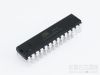
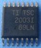
Diagrams