(China (Mainland))

Product Summary
The 74AHCT125PW is a high-speed Si-gate CMOS device and is pin compatible with low power Schottky TTL (LSTTL). The 74AHCT125PW is specified in compliance with JEDEC standard No. 7A.
Parametrics
74AHCT125PW absolute maximum ratings: (1)DC supply voltage: -0.5 +7.0 V; (2)Input voltage range: -0.5 +7.0 V; (3)DC input diode current VI < -0.5 V; note 1: -20 mA; (4)DC output diode current VO < -0.5 V or VO > VCC + 0.5 V; note 1: ±20 mA; (5)DC output source or sink current -0.5 V < VO < VCC + 0.5 V: ±25 mA; (6)DC VCC or GND current: ±75 mA; (7)Storage temperature range: -65 +150 °C; (8)Power dissipation per package for temperature range: -40 to +125 °C; note 2: 500 mW.
Features
74AHCT125PW features: (1)ESD protection: HBM EIA/JESD22-A114-A exceeds 2000 V; MM EIA/JESD22-A115-A exceeds 200 V; CDM EIA/JESD22-C101 exceeds 1000 V; (2)Balanced propagation delays; (3)All inputs have Schmitt-trigger actions; (4)Inputs accepts voltages higher than VCC; (5)For AHC only: operates with CMOS input levels; (6)For AHCT only: operates with TTL input levels; (7)Specified from -40 to +85 and +125 °C.
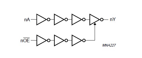
Diagrams
| Image | Part No | Mfg | Description |  |
Pricing (USD) |
Quantity | ||||||||||||
|---|---|---|---|---|---|---|---|---|---|---|---|---|---|---|---|---|---|---|
 |
 74AHCT125PW,112 |
NXP Semiconductors |
Buffers & Line Drivers QUAD 3-STATE BUS BUF |
Data Sheet |
|
|
||||||||||||
|
74AHCT125PW,118 |
NXP Semiconductors |
Buffers & Line Drivers QUAD 3-STATE BUS BUF |
Data Sheet |
|
|
||||||||||||
|
74AHCT125PW-T |
NXP Semiconductors |
Buffers & Line Drivers QUAD 3-STATE BUS BUF |
Data Sheet |
Negotiable |
|
||||||||||||