(China (Mainland))

Product Summary
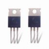
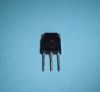
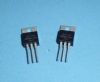
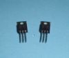
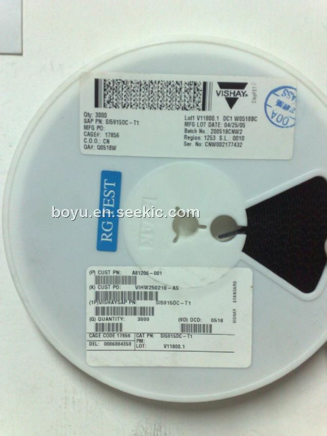
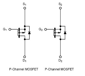
The SI5915DC-T1 is a Dual P-Channel 1.8-V (G-S) MOSFET. The applications of the SI5915DC-T1 include Load Switch and PA Switch for Portable Devices.
Parametrics
SI5915DC-T1 absolute maximum ratings: (1)Drain-Source Voltage VDS : 8V; (2)Gate-Source Voltage VGS: ±8V; (3)Continuous Drain Current (TJ = 150℃): -4.6 to 3.4A; (4)Pulsed Drain Current IDM: -10A; (5)Continuous Source Current (Diode Conduction)a IS : -1.8 to -0.9A; (6)Maximum Power Dissipationa TA = 25℃ PD: 2.1 to 1.1W; (7)Operating Junction and Storage Temperature Range TJ, Tstg: -55 to 150℃; (8)Soldering Recommendations (Peak Temperature): 260℃.
Features
SI5915DC-T1 features: (1)TrenchFET Power MOSFET; (2)Low Thermal Resistance; (3)40% Smaller Footprint Than TSOP-6.
Diagrams
| Image | Part No | Mfg | Description |  |
Pricing (USD) |
Quantity | ||||
|---|---|---|---|---|---|---|---|---|---|---|
 |
 SI5915DC-T1-E3 |
Vishay/Siliconix |
MOSFET 8.0V 4.6A 2.1W 70mohm @ 4.5V |
Data Sheet |
Negotiable |
|
||||
 |
SI5915DC-T1-GE3 |
|
MOSFET 2P-CH 8V 3.4A 1206-8 |
Data Sheet |
Negotiable |
|
||||