(China (Mainland))


Product Summary
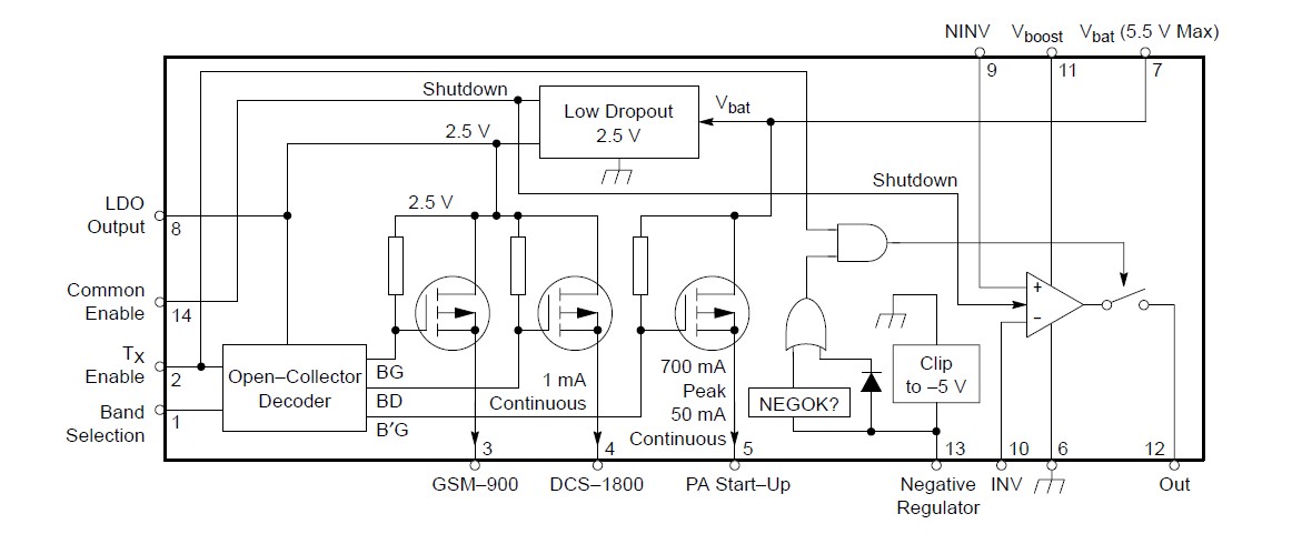
The MC33170DTBR2 is a complete solution for drain modulated dual–band GSM 900MHz and DCS–1800MHz Power Amplifiers. Thanks to its internal decoder, the MC33170DTBR2 drastically simplifies the interface between the PAs and the baseband logic section, providing an immediate gain in part count but also in occupied copper area. The device is also ready for 1V platforms since it accepts logic high control signals down to 900mV 25°C.
Parametrics
MC33170DTBR2 absolute maximum ratings: (1)Band se!ection: 0 to 5.5 V; (2)Tx Enawe: 0 to 5.5 V; (3)GSM-SOO: -5 to 5.5 V; (4)DCS-1800: -5 to 5.5 V; (5)PASM-up: 0 to 5.5 V; (6)VDat: 0 to 5.5 V; (7)NINV: 0 to 5.5 V; (8)INV: 0 to 5.5 V; (9)Boost vcxtage: 0 to 12 V; (10)Negative regulation pin: -5.4 to 5.5 V; (11)Common Enable: 0 to 5.5 V; (12)ESD capabiity. HBM model: 2 kV; (13)ESD capaDHty. Machine rrxxfci: 200 V; (14)Steeflng Syntcn. corcnuous output current : 1 mA; (15)Steeflng Sviitcn. continuous output current : 50 mA; (16)Steering Svincft. peak output current < 1 μs: 700 mA; (17)Maximum power dissipaeon: 500 mw; (18)NWsumx. p<as:te package Tj=25°C: 200 mw; (19)nw suffix p<as:te package Tj=85°C: 200 °C/w; (20)Operating Ambiwent Temperature: -40 to+85 °C; (21)Waximum Jinccon Temperature: 150 °C; (22)Maximum Opefathg JuoctJon Terrpefature: 125 °C; (23)Storage Tempefature Range: -60 to +150°C.
Features
MC33170DTBR2 features: (1)1V platform compatible: ON voltage = 900mV, OFF voltage = 300mV max; (2)Priority management system prevents power modulation before negative bias establishes; (3)High performance 4.5MHz gain–bandwidth product operational amplifier; (4)Drives N or P–channel MOSFET; (5)2.5V low–noise LDO; (6)Idle mode input for very low power consumption (standby mode).
Diagrams