(China (Mainland))

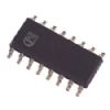
Product Summary
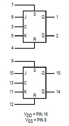
The MC14027BFL1 is a dual J–K flip–flop. It has independent J, K, Clock (C), Set (S) and Reset (R) inputs for each flip–flop. The device may be used in control, register, or toggle functions.
Parametrics
MC14027BFL1 absolute maximum ratings: (1)VDD DC Supply Voltage: -0.5 to + 18.0 V; (2)Vin, Vout Input or Output Voltage (DC or Transient): -0.5 to VDD + 0.5 V; (3)lin, lout Input or Output Current (DC or Transient), per Pin: ±10 mA; (4)PD Power Dissipation, per Packag: 500 mW; (5)Tstg Storage Temperature: -65 to + 150 ℃; (6)TL Lead Temperature (8-Second Soldering): 260 ℃.
Features
MC14027BFL1 features: (1)Diode Protection on All Inputs; (2)Supply Voltage Range = 3.0 Vdc to 18 Vdc; (3)Logic Swing Independent of Fanout; (4)Logic Edge-locked Flip-lop Design-Logic state is retained indefinitely with clock level either high or low; information is transferred to the output only on the positive-going edge of the clock pulse; (5)Capable of Driving Two Low-power TTL Loads or One Low-power Schottky TTL Load Over the Rated Temperature Range; (6)Pin-for-pin Replacement for CD4027B.
Diagrams