(China (Mainland))


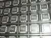
Product Summary
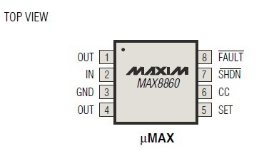
The max8860esa3.3 low-noise, low-dropout linear regulator operates from a +2.5V to +6.5V input and is guaranteed to deliver 300mA. Typical output noise for the max8860esa3.3 is 60μVRMS, and typical dropout is 105mV at 200mA. Designed with an internal P-channel MOSFET pass transistor, the max8860esa3.3 has a low 120μA supply current. An output fault-detection circuit indicates loss of regulation. Applications are (1)Wireless Handsets; (2)DSP Core Power; (3)PCMCIA Cards; (4)Hand-Held Instruments; (5)Palmtop Computers; (6)Electronic Planners.
Parametrics
max8860esa3.3 absolute maximum ratings: (1)IN, SHDN to GND : -7V to +7V; (2)SHDN to IN : -7V to +0.3V; (3)SET, CC, FAULT to GND: -0.3V to +7V; (4)OUT to GND : -0.3V to (VIN + 0.3V); (5)FAULT Sink Current : 20mA; (6)Continuous Output Current : 330mA; (7)Output Short-Circuit Duration : Continuous; (8)Continuous Power Dissipation (TA = +70°C)8-Pin μMAX (derate 4.1mW/°C above +70°C): 330mW; (9)Operating Temperature Range: -40°C to +85°C; (10)Junction Temperature: +150°C; (11)Storage Temperature Range : -65°C to +150°C; (12)Lead Temperature (soldering, 10sec): +300°C.
Features
max8860esa3.3 features: (1)High Output Current (300mA); (2)Low Output Voltage Noise: 60μVRMS; (3)Low 105mV Dropout at 200mA Output; (4)Low 120μA No-Load Supply Current; (5)Thermal-Overload and Short-Circuit Protection; (6)Reverse Battery Protection; (7)10nA Logic-Controlled Shutdown; (8)FAULT Indicator; (9)Small, Space-Saving μMAX Package (1.1mm max height); (10)Small 2.2μF Output Capacitor Saves Space and Cost.
Diagrams