(China (Mainland))


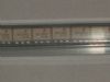
Product Summary
The fa5500an-d1-te1 is a control IC for a power factor correction system. This IC uses a CMOS device with high dielectric strength (30V) to implement low power consumption. The fa5500an-d1-te1 uses the average current control system to ensure stable operation. With this system, a power factor of 99% or better can be achieved.
Parametrics
fa5500an-d1-te1 absolute maximum ratings: (1)Supply Voltage, VC pin, VC: Vcc V; (2)VCC pin Low impedance source (Icc>15mA), VCC1: 30 V; (3)VCC pin Internal zener clamp voltage (Icc<15mA), VCC2: Self Limiting V; (4)Output peak current, IOUT: ±1.5 A; (5)SYNC, VIN-,VDET and OVP pins Input voltage, VSYNC/VVIN-VVDET/VOVP: -0.3 to 5.0 V; (6)IDET pin input voltage, VIDET: -10 to 5.0 V; (7)ON/OFF pin input voltage, VON/OFF: -0.3 to Vcc V; (8)REF pin source current, IREF: -10 mA; (9)Power dissipation (Ta=25℃) DIP-16, Pd: 850 mW; SOP-16: 650 mW; (10)Ambiance temperature, Ta: -30 to +105℃; (11)Maximum junction temperature, Tj: +150℃; (12)Storage temperature, Tstg: -40 to +150℃.
Features
fa5500an-d1-te1 features: (1)Low current consumption by CMOS process; (2)Stand-by: 3μA(max), Start-up: 30μA(max), Operating: 4mA(typ); (3)Good regulation of PFC output voltage from no-load to full-load; (4)Drive circuit for connecting a power MOSFET(IOUT = ±1.5A); (5)Pulse-by-pulse overcurrent and overvoltage limiting function; (6)±2% accuracy reference voltage for setting DC output and overvoltage protection; (7)Output ON/OFF control function by external signal; (8)External synchronizing input pin for synchronous operation with other circuits; (9)Undervoltage lockout function (ON: 16.5V, OFF: 8.9V); (10)16-pin package (DIP/SOP).
Diagrams