(China (Mainland))

Product Summary
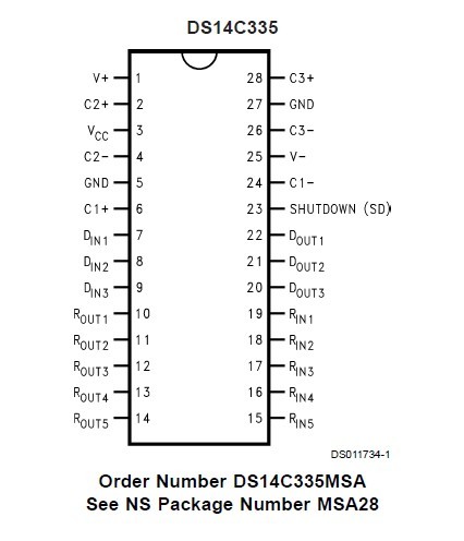
The ds14c335msax is three driver, five receiver device which conforms to TIA/EIA-232-E and CCITT V.28 standard specifications. The ds14c335msax employs an internal DC-DC converter to generate the necessary output levels from a +3.3V power supply. A SHUTDOWN (SD) mode reduces the supply current to 10 μA maximum. In the SD mode, one receiver is active, allowing ring indicator (RI) to be monitored. PC Board space consumption is minimized by the availability of Shrink Small Outline Packaging (SSOP).
Parametrics
ds14c335msax absolute maximum ratings: (1)Supply Voltage (VCC): -0.3V to + 6V; (2)Input Voltage (DIN, SD): -0.3V to + 5.5V; (3)Driver Output Voltage: (V+ + 0.3V)to (V- -0.3V); (4)Receiver Input Voltage: ±25V; (5)Receiver Output Voltage: -0.3V to (VCC+ 0.3V); (6)Junction Temperature: +150°C; (7)Storage Temperature Range: -65°C to +150°C; (8)Lead Temperature (Soldering 4 sec.): +260°C; (9)Maximum Package Power Dissipation @ +25°C SSOP MSA Package: 1286 mW.
Features
ds14c335msax features: (1)Conforms to TIA/EIA-232-E and CCITT V.28 specifications; (2)Operates with single +3.3V power supply; (3)Low power requirement—ICC 20 mA maximum; (4)SHUTDOWN mode—ICX 10 μA maximum; (5)One Receiver (R5)active during SHUTDOWN; (6)Operates up to 128 kbps—Lap-Link Compatible; (7)Flow through pinout; (8)4V/μs minimum Slew Rate guaranteed; (9)Inter-operates with +5V UARTs; (10)Available i28-lead SSOP EIAJ Type II package.
Diagrams
| Image | Part No | Mfg | Description |  |
Pricing (USD) |
Quantity | ||||||||
|---|---|---|---|---|---|---|---|---|---|---|---|---|---|---|
 |
 DS14C335MSAX |
National Semiconductor (TI) |
Bus Receivers |
Data Sheet |
|
|
||||||||
 |
DS14C335MSAX/NOPB |
National Semiconductor (TI) |
Bus Receivers |
Data Sheet |
|
|
||||||||