(China (Mainland))

Product Summary
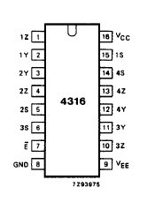
The 74hc4316n is a high-speed Si-gate CMOS device. The 74hc4316n is specified in compliance with JEDEC standard no. 7A. The 74hc4316n has four independent analog switches. Each switch has two input/output terminals (nY, nZ) and an active HIGH select input (nS). When the enable input (E) is HIGH, all four analog switches are turned off. Applications are (1)Signal gating; (2)Modulation; (3)Demodulation; (4)Chopper.
Parametrics
74hc4316n absolute maximum ratings: (1)VCC DC supply voltage: -0.5 to +11.0 V; (2)±IIK DC digital input diode current: 20 mA for VI < -0.5 V or VI > VCC + 0.5 V; (3)±ISK DC switch diode current: 20 mA for VS < -0.5 V or VS > VCC + 0.5 V; (4)±IS DC switch current: 25 mA for -0.5 V < VS < VCC + 0.5 V; (5)±IEE DC VEE current: 20 mA; (6)±ICC; ±IGND DC VCC or GND current: 50 mA; (7)Tstg storage temperature range: -65 to +150 °C; (8)Ptot power dissipation per package for temperature range: -40 to +125 °C; (9)plastic DIL: 750 mW above +70 °C: derate linearly with 12 mW/K; (10)plastic mini-pack (SO): 500 mW above +70 °C: derate linearly with 8 mW/K; (11)PS power dissipation per switch: 100 mW.
Features
74hc4316n features: (1)Low ON resistance: 160 W (typ.)at VCC - VEE = 4.5 V, 120 W (typ.)at VCC - VEE = 6.0 V, 80 W (typ.)at VCC - VEE = 9.0 V; (2)Logic level translation: to enable 5 V logic to communicate with ± 5 V analog signals; (3)Typical break before make built in; (4)Output capability: non-standard; (5)ICC category: MSI.
Diagrams
| Image | Part No | Mfg | Description |  |
Pricing (USD) |
Quantity | ||||||||||||
|---|---|---|---|---|---|---|---|---|---|---|---|---|---|---|---|---|---|---|
 |
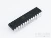
 74HC4316N |
NXP Semiconductors |
Analog Switch ICs QUAD BILATRL ANALOG SWITCH |
Data Sheet |
Negotiable |
|
||||||||||||
|
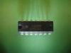
74HC4316N,652 |
NXP Semiconductors |
Analog Switch ICs QUAD BILATRL ANALOG |
Data Sheet |
|
|
||||||||||||